Solid State Institute
Lead Free Perovskites
Engineering bright Lead-free double perovskites nanoparticles
Lead halide perovskites are considered future material favorites due to their high efficiency in optoelectronic applications. However, lead is a toxic substance banned by many industries. We are replacing lead in perovskites with less toxic materials, for example a combination of silver and Indium instead of two lead atoms.
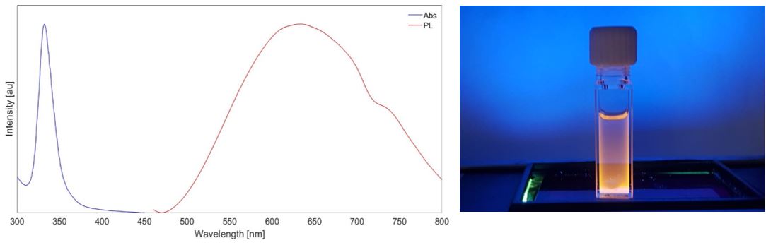
In this project our goal is to engineer lead free emissive nanoparticles for next generation display and lighting applications. We achieve this by using sodium alloying and bismuth doping to a silver-indium double perovskite nanoparticle. This material engineering enables control of a self-trapped-exciton affecting the absorption and emission intensity and wavelength. As seen in the photoluminescence spectrum and in the photo, the resulting nanocrystals are very bright.
Transmission electron microscopy and High Angle Annular Dark Field STEM Energy dispersive X-ray spectroscopy mapping
We study the structure of Cs2AgInCl6 perovskite materials, using Scanning Transmission Electron Microscopy (STEM) diffraction and X-ray diffraction techniques. Using this method, we determine the composition of double perovskite nanocrystals with sub nanometer resolution. This allows us to determine what chemicals are present in the particles (Cs,Ag,In,Cl), and to further engineer their properties.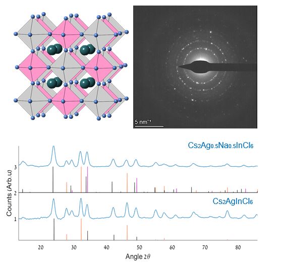 Then, we can study Cs2AgInCl6 perovskite nanocubes void defect dynamics by Transmission Electron Microscopy technique at atomic resolution.
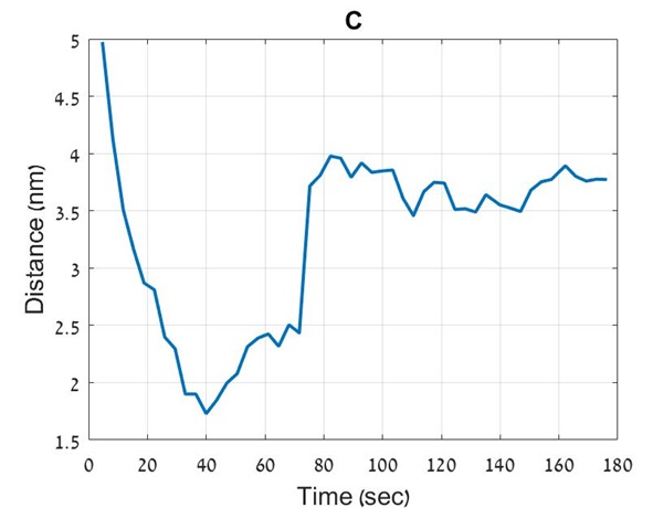
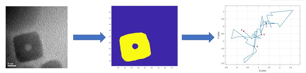
Using image processing, we are able to create a map of the trajectory of a nanovoid within the Perovskite nanocube. This allow us to make sense of the dynamics of the system.
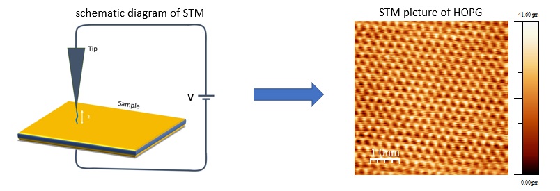
Scanning Tunneling Microscope (STM)
In a Scanning Tunneling microscope, we bring a sharp tip within a small distance from the sample. We then apply a voltage and use the tunneling current to characterize the sample. This technic will allow us to study our materials with nanoscale precision, and uncover the close relationship between the crystal size and its energy levels.
Under the influence of an electron beam, voids are generated within the nanocube (A). Using image processing, we can create a binary image (B) that captures only the nanocube and the void inside it. This allow us to make sense of the dynamics of the system and make it easier to calculate relevant quantities, like the position of the void relative to the crystal center (C).